Key Points
- Researchers from Fudan University have developed a flexible “fiber chip” by embedding large-scale integrated circuits (ICs) directly into soft, elastic polymer fibers, a breakthrough published in Nature on January 22, 2026.
- The innovation utilizes a multi-layer stacked architecture that spirals deep within the fiber, enabling a component density of 100,000 units (transistors, capacitors, etc.) per centimeter.
- These fiber chips can perform both digital and analog circuit computations while retaining the fiber’s natural flexibility, fundamentally shifting wearable electronics from rigid attachments to fully integrated computing within textiles.
- This technology has significant implications for smart fabrics, real-time health monitoring, protective gear, and IoT applications, allowing garments to become computational hardware.
- The development marks a crucial step in China’s push in advanced materials and novel computing architectures, offering a solution to the “form factor problem” in integrating computing into unconventional places.
- Smart Fabrics: Real-time health monitoring (heart rate, temperature).
- Protective Gear: Integration into exoskeletons and military uniforms.
- Flexible Displays: Screens woven directly into textile surfaces.
- IoT Nodes: Fibers acting as intelligent network communication points.

The future of computing just got a lot more flexible.
Researchers from Fudan University (Fudan Daxue 复旦大学) have pulled off something that sounded like science fiction just a few years ago: they’ve successfully embedded large-scale integrated circuits (ICs) directly into soft, elastic polymer fibers.
This isn’t a marginal improvement—it’s a fundamental shift in how we think about computing hardware.
The breakthrough was published in the prestigious international journal Nature on January 22, 2026, and it’s already turning heads in the tech and semiconductor world.
From Theory to Reality: The Fiber Chip Innovation
For years, researchers have theorized about embedding computing power into fabrics and fibers.
The challenge?
Making it actually work—at scale, and without destroying the fiber’s natural flexibility.
The Fudan University team, led by Peng Huisheng (Peng Huisheng 彭慧胜) and Chen Peining (Chen Peining 陈培宁), decided to tackle this head-on by rethinking the entire architecture.
Find Top Talent on China's Leading Networks
- Post Across China's Job Sites from $299 / role
- Qualified Applicant Bundles
- One Central Candidate Hub
Your First Job Post Use Checkout Code 'Fresh20'
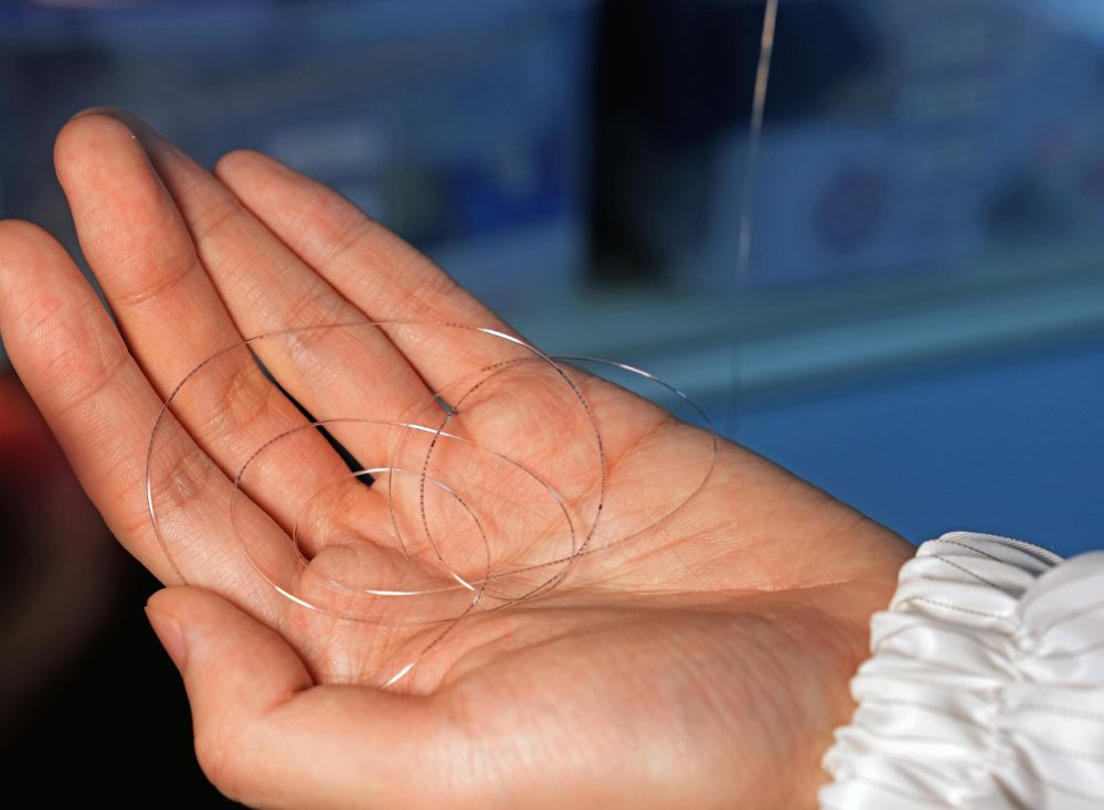
A “fiber chip” photographed on January 19. (Photo by Liu Ying, Xinhua News Agency)
ExpatInvest China
Grow Your RMB in China:
- Invest Your RMB Locally
- Buy & Sell Online in CN¥
- No Lock-In Periods
- English Service & Data
- Start with Only ¥1,000

Breaking the Traditional Design: Multi-Layer Spiral Architecture
Here’s where the innovation gets interesting.
Most chip designers think in 2D—they focus on maximizing the surface area of a substrate.
The Fudan team thought differently.
Instead of building circuits on the fiber’s surface, they designed a multi-layer stacked architecture that spirals deep within the fiber itself.
Think of it like this: rather than painting circuits on the outside of a rope, they’re building them inside, layer upon layer, in a helical pattern.
This approach maximizes the internal space—something traditional fiber electronics couldn’t do.
The technical challenge was enormous.
The team spent years developing a fabrication process capable of performing high-density lithography directly on elastic polymers.
Lithography is the core technology used to etch circuits onto semiconductors, but doing it on soft, stretchable materials is a completely different ball game.

Resume Captain
Your AI Career Toolkit:
- AI Resume Optimization
- Custom Cover Letters
- LinkedIn Profile Boost
- Interview Question Prep
- Salary Negotiation Agent
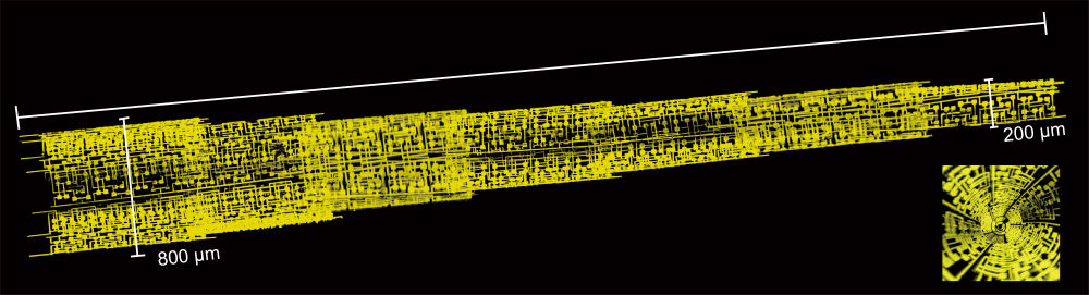
Structural diagram of the multi-layer integrated circuit inside the fiber. (Courtesy of Fudan University)
The Numbers: Integration Density and Computing Power
So what did they actually achieve?
The lab results are impressive.
The team has already achieved preliminary large-scale preparation of these fiber chips, and the density of electronic components (transistors, capacitors, etc.) inside the fibers has reached 100,000 units per centimeter.
To put that in perspective: that’s serious integration density packed into an incredibly small space.
By efficiently interconnecting these transistors with other electronic components, the fibers can now perform both digital and analog circuit computations.
In other words: they’re not just flexible fibers anymore—they’re computing devices that happen to be woven into fabric.
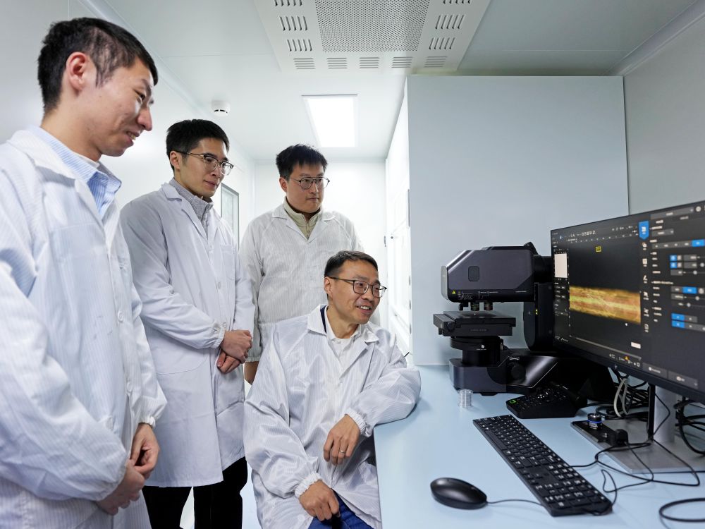
The “Fiber Chip” research team photographed on January 19. (Photo by Liu Ying, Xinhua News Agency)
Why This Matters: Applications and Industry Impact
The implications here are genuinely significant.
This technology opens doors to wearable electronics that are truly integrated into clothing and textiles, not just stuck on top as an afterthought.
Potential applications include:
- Smart fabrics that monitor health metrics in real-time (heart rate, body temperature, muscle activity)
- Embedded computing in protective gear (think exoskeletons, military uniforms, emergency responder suits)
- Flexible displays woven directly into textiles
- Energy harvesting systems built into clothing
- IoT applications where fibers themselves become intelligent network nodes
What makes this different from existing smart textiles?
Most current smart fabrics attach rigid chips to cloth using conductive threads or patches.
This fiber chip technology fully integrates computing power into the fiber itself, meaning the entire garment becomes computational hardware while maintaining its natural properties—it stretches, it bends, it feels like fabric.
Expert Perspective: What Industry Leaders Are Saying
Tao Guangming (Tao Guangming 陶光明), a professor at Huazhong University of Science and Technology (Huazhong Keji Daxue 华中科技大学) and leading expert in fiber electronics, had this to say:
“This new fabrication route grants fibers information processing capabilities while maintaining their inherent softness. It not only opens a new path for fiber electronic system integration but also offers potential new directions for the broader evolution of the integrated circuit industry.”
Translation: this isn’t just a materials science breakthrough—it could reshape how the entire semiconductor industry thinks about integration and form factor.
For context, the IC industry has been obsessed with two trends for decades: miniaturization (making chips smaller) and density (fitting more onto the same footprint).
Fiber chips add a third dimension: they solve the “form factor problem”—how do you integrate computing into places where rigid silicon simply can’t go?
What’s Next for Fiber Chip Technology?
The research is still in its early stages.
The team has achieved “preliminary large-scale preparation” in the lab, which means they’ve proven the concept works, but scaling production and optimizing the process for commercial applications will take time.
Key challenges ahead likely include:
- Scaling manufacturing from lab batches to commercial production
- Improving thermal management (heat dissipation in a fiber is different than in traditional chips)
- Developing standardized testing and quality control for fiber chips
- Creating supply chain and assembly infrastructure
- Addressing power delivery in wearable applications
But the foundational technology is proven.
That’s the big deal here.
The Broader Context: China’s Advanced Materials Push
This breakthrough is part of a larger trend in Chinese tech.
While the US and Europe have traditionally dominated semiconductor research, China is making serious moves in advanced materials and novel computing architectures.
Fiber chips fit squarely into this strategy because they represent a completely different approach to computing—not just incremental improvements to silicon wafers, but fundamental rethinking of form factors and integration methods.
For investors and founders watching the tech space, this signals that the next generation of hardware innovation might not come from traditional chip foundries, but from materials science labs exploring unconventional substrates and architectures.
Key Takeaways: Flexible “Fiber Chip” Technology
- Fudan University researchers have successfully embedded integrated circuits into soft, elastic polymer fibers
- The breakthrough uses a multi-layer spiral architecture that maximizes internal space rather than relying on surface area alone
- Integration density has reached 100,000 transistors per centimeter, enabling real computing capabilities
- The fibers maintain their natural flexibility while performing digital and analog circuit computations
- Potential applications span smart fabrics, wearable health monitoring, protective gear, and IoT devices
- The research was published in Nature (January 22, 2026) and represents a fundamental shift in how we can integrate computing into everyday materials
- This technology could open entirely new categories of products and reshape thinking in the semiconductor industry
The fiber chip breakthrough from Fudan University demonstrates that the next frontier in computing isn’t about making chips smaller—it’s about making them more flexible, literally.